


Plastic substrate will be replaced with glass substrate for future semiconductor chips, and Samsung wants to create an ecosystem for it.
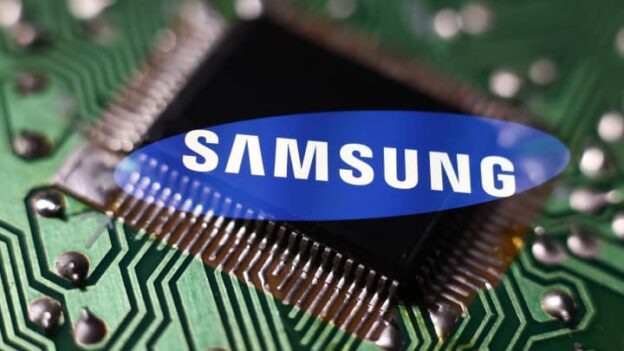
Samsung is a key player in the semiconductor chip technology space. It not only designs memory and logic chips but also manufactures them for several other brands. A substrate is the foundation upon which a semiconductor chip is fabricated, and Samsung Electro-Mechanics aims to upgrade it for future chips.
Samsung aims to upgrade to glass substrates for future semiconductor chips
Samsung Electro-Mechanics said it is building a glass substrate ecosystem for semiconductor chips and it aims to quickly solve technological challenges related to it and commercialize the technology. This is the first time Samsung disclosed its glass substrate plans.
Currently, plastic wafers are used as substrates for semiconductor chips, and it will soon be replaced by glass substrates. Compared to chips using plastic substrate, those with glass substrate will reportedly have improved performance and lower the power consumption.

At an event titled ‘Electronic Times Tech Day: All About Glass Substrates,’ held at POSCO Tower Yeoksam in Seoul earlier this week, Joo Hyuk, VP of Samsung Electro-Mechanics Research Institute, said, “We plan to establish a consortium with several suppliers and technology partners to create a semiconductor glass substrate ecosystem.“
Over 250 people from academia, executives of related firms, and researchers attended the event.
The company will create an ecosystem of equipment (SBOJ), materials, parts, and process brands and co-operation between them. While the company didn’t disclose the actual timeframe, Samsung Electro-Mechanics is reportedly already in discussions with related firms, and the ecosystem will be launched soon.
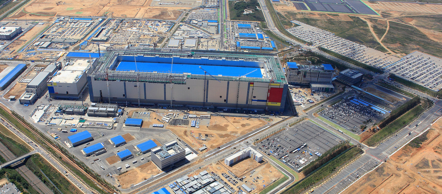
A pilot process could start at the company’s production line at its plant in Sejong, South Korea, in the second quarter of this year followed by mass production after 2027. This accelerated move comes as a result of the recent explosive demand for AI chips.
Samsung Electro-Mechanics is reportedly in talks with Samsung Semiconductor, which designs (System LSI) and manufactures (Samsung Foundry) chips, and other global chip firms, including Intel, Nvidia, and Qualcomm.
Glass substrate is said to have lower warpage, so it is easier to implement precise signal paths, resulting in higher performance. It also allows printing a large number of copper passages, resulting in high power efficiency.
The company is targeting both glass interposer (intermediate material) and glass core (primary material) markets. Glass core connects the GPU with high-bandwidth memory (HBM) in AI chips, like the ones from AMD and Nvidia.