


International Business Machines Corp (NYSE:IBM) unveiled new semiconductor technology featuring a sub-1 nanometer chip architecture, which Wedbush analysts see as a significant step in chip scaling as demand for artificial intelligence computing continues to grow.
IBM said the sub-1 nm design incorporates approximately 100 billion transistors on a chip roughly the size of a fingernail, which the analysts noted is about twice the density of the company’s current 2 nm technology. The architecture is based on a 3D “nanostack” approach that vertically layers and staggers transistors in order to increase density and improve performance efficiency.
According to Wedbush analysts, the new design is intended to deliver up to 50% higher performance or up to 70% better energy efficiency compared with IBM’s 2 nm chips. They wrote that these improvements could support workloads across generative AI, cloud infrastructure, and next-generation electronic devices, where demand for processing power and energy efficiency continues to rise.
The analysts also highlighted that IBM demonstrated a 40% scaling improvement in SRAM using the nanostack architecture, which they wrote could enable chip designers to build more efficient processors capable of handling higher-bandwidth data flows associated with AI applications.
Wedbush analysts wrote that IBM continues to position itself as a key player in advanced semiconductor development, with efforts spanning silicon design, AI-focused hardware, logic systems, and quantum computing. They noted that the company is working with a range of industry partners, including ASML on advanced lithography techniques, as well as Lam Research, Tokyo Electron, and SCREEN Semiconductor Solutions, to support high numerical aperture EUV processes and related tooling.
The analysts wrote that these partnerships have contributed to early-stage working devices and reflect IBM’s ongoing efforts in advanced process development aimed at extending its semiconductor roadmap over the next decade. They added that the company’s progress in lithography and transistor architecture could strengthen its positioning in AI-related hardware markets.
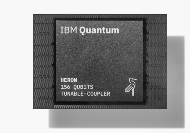
In addition to its semiconductor developments, IBM announced plans to establish a standalone quantum foundry business called Anderon. Wedbush analysts wrote that the entity is intended to leverage IBM’s existing expertise in quantum computing and semiconductor technologies to support domestic quantum wafer manufacturing capabilities.
The analysts added that IBM has outlined a potential timeline for early adoption of its nanostack technology at sub-1 nm nodes, with a possible production pathway for the quantum-focused facility within the next five years.
Wedbush analysts wrote that IBM’s broader quantum strategy remains focused on providing infrastructure and runtime environments for quantum computing applications, positioning the company as a long-term provider of foundational technologies in the sector.
Wedbush maintains an ‘Outperform’ rating on the stock with a $350 price target, implying upside from current levels of about $258.
https://ca.finance.yahoo.com/news/ibm-quantum-foundry-plan-adds-173000743.html