


Arriving First With Its Feynman GPUs
NVIDIA’s Feynman GPUs will be the first to feature Co-Packaged Optics, but this wasn’t always the case until the AI giant decided to switch gears.
Co-Packaged Optics Were Many Years Away, But NVIDIA Decided To Move Ahead With Its Feynman GPUs
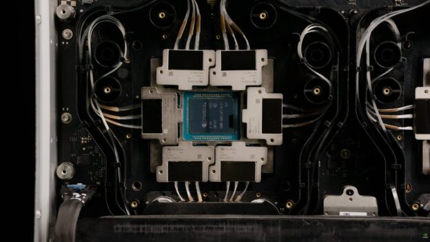
CPO or Co-Packaged Optics (Silicon Photonics) is the next-generation solution that reduces reliance on copper and harnesses light to transfer signals. These CPOs are packaged alongside hardware accelerators such as GPUs and will be a key solution for next-gen AI factories, offering improved interconnect latency and creating high-bandwidth connections between CPU and GPU.
If we go by the original plans, CPO was originally slated for commercialization by 2033, but NVIDIA fast-forwarded the optics roadmap by 5 years, bringing it forward in 2028 with its next-gen Feynman GPUs. The report from Nikkei Xtech states that as AI firms scale out, distances between installed platforms can reach north of 10km, and data will need to be transmitted fast at several hundred Gigabits per second or more. Traditional methods make this difficult, & that’s where optics replace copper cables as the primary means to transfer data.

As such, the Optical Compute Interconnect Multi-Source Agreement (OCI-MSA) announced the establishment back in March, involving major AI firms such as NVIDIA, Broadcom, AMD, Meta, OpenAI, and Microsoft. NVIDIA, being the largest of the bunch, is bringing out its first Co-Packaged solution with Feynman GPUs in 2028.
At GTC 2026, NVIDIA confirmed that its Feynman GPUs will adopt 3D Die Stacking technology. With 3D Die Stacking, we could very well see the first use of 3D stacked GPU dies from NVIDIA. It also looks like NVIDIA will utilize Intel as a Foundry partner and leverage their advanced packaging technologies, such as EMIB, to produce Feynman chips.
The other exciting announcement is that instead of next-gen HBM, NVIDIA is now listing custom HBM tech for its Feynman GPUs. With Rubin leveraging HBM4 and Rubin Ultra leveraging HBM4E, it looks like NVIDIA’s solution might be either a custom or heightened version of HBM4E or a custom HBM5 solution, which makes them stand out from the standard HBM5 offerings.

NVIDIA is also confirming the name of its next-gen Data Center CPU architecture. Feynman isn’t going to rely on Vera; it is going to use a brand new CPU called Rosa, which is named after American physicist & a Nobel Prize winner, Rosalyn Sussman. No details are mentioned yet, but given NVIDIA’s trajectory, we can expect some big improvements.
Besides this, NVIDIA will continue to roll out a full spectrum of chips for its AI platforms, such as BlueField-5, NVLink 8 CPO, Spectrum 7 204T, CPO, and CX10. As expected, NVIDIA’s Rosa Feynman solutions will be arriving in 2028. AMD is also reportedly working on its own Co-Packaged Optics with Global Foundries and is expected to see the first implementation with MI500 GPUs around a similar 2028 timeline.
NVIDIA Data Center / AI GPU Roadmap
| GPU Codename | Feynman | Rubin (Ultra) | Rubin | Blackwell (Ultra) | Blackwell | Hopper | Ampere | Volta | Pascal |
|---|---|---|---|---|---|---|---|---|---|
| GPU Family | GF200? | GR300? | GR200? | GB300 | GB200/GB100 | GH200/GH100 | GA100 | GV100 | GP100 |
| GPU SKU | F200? | R300? | R200? | B300 | B100/B200 | H100/H200 | A100 | V100 | P100 |
| Process Tech | TSMC A16? | TSMC N2P? | TSMC N3P? | TSMC 4NP | TSMC 4NP | TSMC 5nm | TSMC 7nm | TSMC 12nm | TSMC 16nm |
| CPU | Rosa | Vera | Vera | Grace | Grace | Grace | N/A | N/A | N/A |
| Memory | HBM4e/HBM5? | HBM4 | HBM4 | HBM3e | HBM3e | HBM2e/HBM3/HBM3e | HBM2e | HBM2 | HBM2 |
| Launch | 2028 | 2027 | 2026 | 2025 | 2024 | 2022-2024 | 2020-2022 | 2018 | 2016 |

 About the author: A Software Engineer by training and a PC enthusiast by passion,
https://wccftech.com/nvidia-fast-forwarded-co-packaged-optics-five-years-ahead-arriving-with-feynman-gpus/amp/