The AI super-cycle is expected to deliver transformative growth for our global economy—over $15T and 100M jobs by 2030. To realize this opportunity, we need to lean on the same tools which brought us here: the creative forces of engineering design and scientific discovery. Throughout history, we have built upon the advancements of earlier generations to learn, develop, and invent for the future. Using the latest accelerated compute hardware, we’re seeing remarkable breakthroughs for engineering design and scientific discovery, like a 40X speedup for semiconductor design or greater than 1000X speedup for molecular simulation. Accelerated electronic and system design automation (EDA/SDA) will enable AI to be a transformative force for all, tackling challenges in productivity, power efficiency, and more.

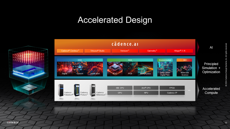
Figure 1: Cadence accelerated design solution
At Cadence, we have been following a simple but powerful recipe to accomplish this—a three-layer cake of AI, physical simulation and optimization, and accelerated compute. Our core competency has always been the middle layer – the accurate simulation and optimization of electronic systems—governed by the laws of physics. This spans from semiconductor design, to 3D-IC advanced packaging, to printed circuit boards, to data centers, and beyond. This middle layer is reinforced and made more powerful by leveraging a foundation of modern accelerated compute in the bottom layer—CPUs, GPUs, and custom bespoke silicon. Accelerated compute enables larger systems and more complex optimizations to be brought to bear that were considered impossible before. It is the key to unlocking the mathematical concepts that were previously discarded because they took too much runtime or memory. Both these layers together are helping create new AI advancements by generating large amounts of high-quality science-based data. All three layers work together to accelerate the engineering design and scientific discovery process.
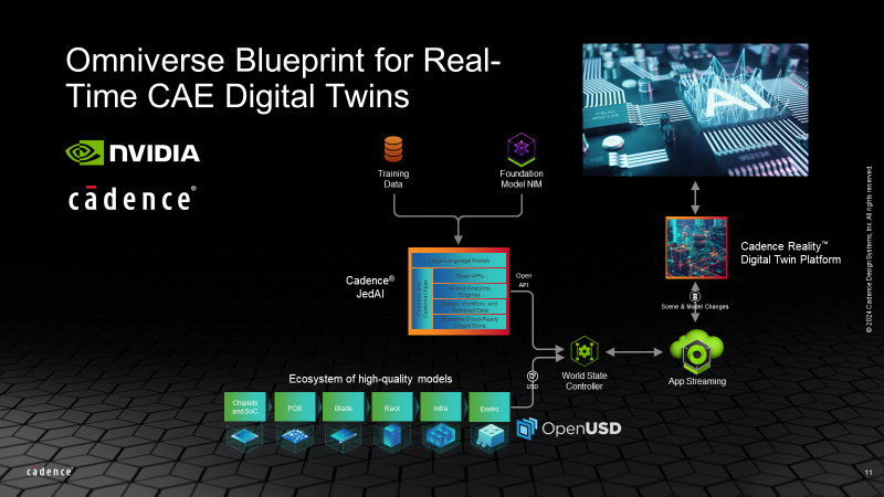
We’ve been collaborating with NVIDIA to co-optimize hardware and software to maximize the benefit of this paradigm. Understanding the benefits and limitations of the hardware and the underlying algorithms is critical to get the most out of accelerated compute. The key for accelerated compute is not treating all hardware like the previous generation’s general-purpose compute and miss opportunities to exploit new compute innovations. The best computer scientists can understand the compute platforms their code is being designed for and use that to target the optimal overall performance. By leaning into each platform’s strengths, matching software to hardware, we’re seeing stunning results. NVIDIA’s Blueprint for real-time computer-aided engineering digital twin helps this process and is being adopted by Cadence software—like our Cadence Reality Digital Twin Platform, and others.

Figure 2: NVIDIA Blueprint and Cadence accelerated design collaboration and solution
Some examples of the benefits we’re seeing from semiconductor design, to data centers, to drug discovery:
- Digital design – 40X speedup for the placement algorithm used in digital design using NVIDIA GPUs. This allows our Cadence Cerebrus Intelligent Chip Explorer’s agentic AI to explore a vast solution space and deliver better silicon more effectively.
- Custom and analog simulation – Up to 10X speedup for Cadence Spectre X using NVIDIA’s GH200 platform, allowing faster analog design iterations and more testing to discover hard to find corner case issues.
- Debug and verification – Over 2X better performance per dollar matching our Xcelium Logic Simulator to the NVIDIA Grace CPU.
- 3D-IC and system design – 14X improvement in our thermal simulations and 5X for stress/warpage using NVIDIA GPUs with our Celsius Studio.
- Multiphysics – Approaching 100X faster CFD simulations using modern GPUs to simulate the design of advanced clean energy technology, and 4X more energy efficient simulations using the NVIDIA Grace CPU when doing meshing for design of automotive and aerospace applications with Cadence Fidelity CFD Platform powered by Omniverse. Accelerated compute is sustainable compute—reducing overall energy consumption and carbon emissions.
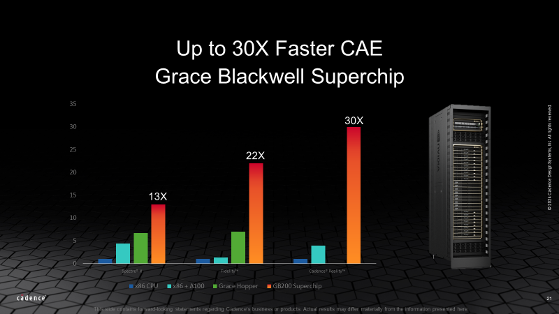
- Data center design and operation – Over 20X speedup moving from general purpose CPUs to NVIDIA GPUs with Cadence Reality Digital Twin Platform. This not only enables faster simulations for digital twins, but it also gives higher-quality visualizations which makes the build out of the AI infrastructure more energy efficient.
- Drug discovery – Benchmarking 1121X more throughput and 15X more cost-efficient drug discovery by leveraging NVIDIA GH200 Grace Hopper Superchip and NVIDIA BioNeMo with Cadence Orion Molecular Design Platform.

Figure 3: Up to 30X faster CAE with the NVIDIA Grace Blackwell Superchip
We live in an era defined by the technology around us and driven by the creative forces of engineering design and scientific discovery. Accelerating these creative forces will unlock new benefits and help all of us realize the benefits from AI. Let’s work together to change the world and even more breakthroughs coming as we update our Cadence platforms to the Blackwell architecture.
https://community.cadence.com/cadence_blogs_8/b/corporate-news/posts/accelerating-design-semiconductors-data-centers-and-sciences?


