


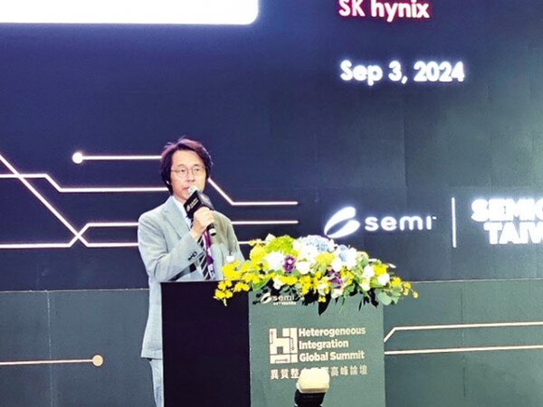
On September 3 (local time), Kangwook Lee, Vice President of SK Hynix Packaging Development, delivered a presentation titled “HBM and Advanced Packaging Technology for the AI Era” at the “Heterogeneous Integration Global Summit 2024” held at the Nangang Exhibition Center in Taipei, Taiwan. The event highlighted SK Hynix’s collaboration with TSMC in the next-generation HBM (High Bandwidth Memory) sector, showcasing the company’s leadership in custom memory for the AI era.
During his presentation, Lee emphasized the increasing importance of heterogeneous integration technology, which integrates semiconductor chips made with different processes into a single package. This technology is crucial for maximizing performance in SK Hynix’s sixth-generation product, HBM4, scheduled for mass production next year. “Current 8-layer and 12-layer HBM3E process over 1.18TB (terabytes) of data per second and support up to 36GB of capacity. HBM4 will be supplied in 12 and 16 layers, with a maximum capacity of 48GB and data processing speeds exceeding 1.65TB per second. By applying logic processes to the base die from HBM4, we expect improvements in performance and energy efficiency,” Lee stated.
SK Hynix and TSMC are collaborating on the development of HBM4, which is scheduled for mass production in 2025. The key to this development is using TSMC’s 5-nanometer process to create the base die at the bottom of the HBM4 package. HBM is created by stacking multiple DRAMs on top of a base die and vertically connecting them using TSV (Through-Silicon Via) technology. The base die is connected to the GPU (Graphics Processing Unit) and controls the performance of the HBM.
Lee also highlighted the advantages of the advanced MR-MUF technology adopted by SK Hynix. “MR-MUF packaging technology allows for low bonding pressure and temperature application and batch heat treatment, offering more than 30% performance advantage in heat dissipation compared to other processes. We are preparing both advanced MR-MUF and hybrid bonding methods for 16-layer products and plan to choose the optimal method that meets customer needs,” he explained.
Currently, SK Hynix is mass-producing HBM3 and HBM3E 8-layer products using MR-MUF technology and 12-layer products using advanced MR-MUF technology. The same technology will be applied to the mass production of HBM4 12-layer products, which are scheduled for shipment in the second half of next year. Additionally, SK Hynix is preparing for the seventh-generation HBM4E, which will follow HBM4.
The demand for HBM in the AI market is also expected to increase significantly. The generative AI market is projected to grow at an average annual rate of 27% from 2023 to 2032, and the HBM market is expected to grow at an average annual rate of 109% from 2022 to 2025. This growth underscores the importance of SK Hynix’s advancements in HBM technology.
Shang Y. Hou, Director of TSMC, also emphasized the growing importance of heterogeneous integration technology due to the increase in AI training applications. “Scaling issues with the size of interposers and package substrates have become inevitable. The next step after packaging 12 HBMs and 9 reticles in Chip on Wafer on Substrate (CoWoS) will be System on Wafer (SoW), which assembles 43 reticles,” Hou said. CoWoS is a 2.5D packaging technology developed by TSMC and is used in NVIDIA’s AI semiconductor packaging.
Meanwhile, Lin Jun-cheng, Vice President of Advanced Packaging Development Team at Samsung Electronics, who previously worked at TSMC, will be a speaker at the Heterogeneous Integration Global Summit on the last day of the SEMICON Taiwan event on September 6. He will explain the 16-layer HBM stacking technology with CoRW hybrid Cu bonding applied in HPC/AI/ML application fields.
출처 : Businesskorea(https://www.businesskorea.co.kr)
https://www.businesskorea.co.kr/news/articleView.html?idxno=224294