


With over 60 EUV machines to be delivered, TSMC is poised to maintain its leadership in semiconductor manufacturing.
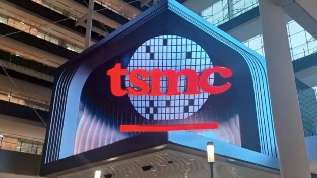
Taiwan Semiconductor Manufacturing Company (TSMC), the world’s largest contract chipmaker, is making significant strides towards its 2nm production capabilities.
With a massive investment exceeding USD 12.3 billion in Extreme Ultraviolet Lithography (EUV) equipment, TSMC is set to begin mass production of its advanced 2nm process in 2025.
TSMC’s investment likely focuses on acquiring more standard EUV machines to bolster their production capacity for the upcoming 2nm process (N2) expected in 2025. This aligns with their strategy of optimizing existing EUV technology for their immediate needs.
This blog post explores the details of TSMC’s investment, the role of key equipment manufacturers, and the broader implications for the semiconductor industry.
Follow us on Linkedin for everything around Semiconductors & AI
Background
TSMC’s advanced processes, like 7nm and 5nm nodes, are widely used in high-performance computing and mobile applications.
As demand for more powerful and efficient chips grows, TSMC focuses on advancing to the 2nm process.

EUV lithography is crucial for achieving smaller, more efficient designs at the 2nm node. This technology uses extreme ultraviolet light to create very fine patterns on silicon wafers. It enables the production of smaller and more powerful chips.
The shift to EUV lithography is a significant technological leap. TSMC fully embraces this to maintain its competitive edge.
EUV Investment:
- Amount: Over USD 12.3 billion (roughly TWD 400 billion)
- Timeline: Deliveries of EUV machines are expected throughout 2024 and 2025 with over 60 units anticipated .
- Significance: This substantial investment highlights TSMC’s commitment to staying ahead in the race for ever-smaller and more powerful chips. EUV technology is crucial for achieving the extreme precision required for 2nm fabrication.
2nm Production:
- Expected Start: Risk production is slated for late 2024, with mass production following in 2025.
- Technology: TSMC’s 2nm process, codenamed N2, will utilize a new “nanosheet transistor” architecture for the first time. This promises significant improvements in performance and power efficiency compared to the previous 3nm generation [https://www.tsmc.com/english/dedicatedFoundry/technology/logic/l_2nm].
- Competition: While TSMC is a leader, other chipmakers like Samsung are also targeting 2nm production around the same timeframe.
Why It Matters
The semiconductor industry is the backbone of modern technology, powering everything from smartphones to data centers. As technology evolves, the demand for faster, more efficient, and more powerful chips continues to grow. Achieving smaller process nodes, such as 2nm, is essential for meeting this demand and driving further advancements in various fields, including artificial intelligence (AI), 5G, and high-performance computing (HPC).
TSMC’s investment in EUV technology and its move towards 2nm production are critical for several reasons:
- Maintaining Leadership: By advancing to the 2nm node, TSMC reinforces its position as a leader in the semiconductor industry. This move ensures that TSMC remains at the forefront of technological innovation, capable of producing the most advanced and efficient chips.
- Meeting Demand: The shift to smaller process nodes allows for the production of chips that are not only more powerful but also more energy-efficient. This is crucial for applications in AI, 5G, and HPC, where performance and efficiency are paramount.
- Economic Impact: TSMC’s investment will have significant economic implications, benefiting the entire semiconductor supply chain. Equipment manufacturers, such as ASML and Gudeng Precision, stand to gain from the increased demand for EUV machines and related technologies.
- Technological Advancements: The move to 2nm and the adoption of EUV lithography will drive technological advancements across various industries. This progress will enable the development of more advanced technologies, enhancing the capabilities of AI, improving the performance of mobile devices, and supporting the growth of data centers.
Read More: Top 7 Semiconductor Companies by Revenue in Q1 2024: Market Share Analysis and Insights – techovedas
TSMC’s Strategic Investment in EUV
TSMC’s ambitious plan to mass-produce 2nm chips by 2025 is underpinned by a substantial investment in EUV technology.
According to a report from Commercial Times, TSMC will receive over 60 EUV machines in 2024 and 2025, with a total investment surpassing TWD 400 billion (approximately USD 12.3 billion).
This investment underscores TSMC’s commitment to maintaining its technological edge in semiconductor manufacturing.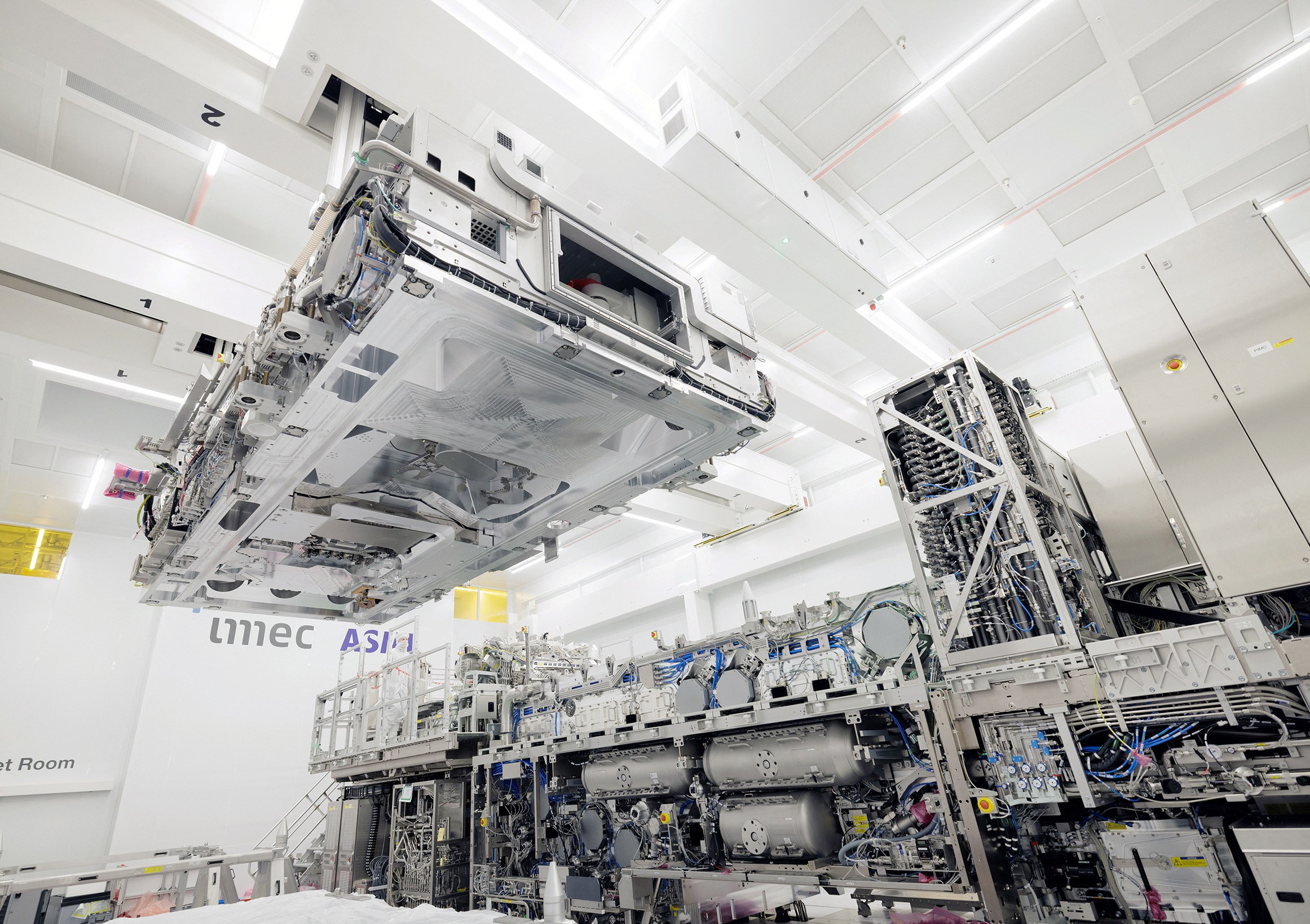
EUV lithography, essential for advanced semiconductor processes, allows for the creation of smaller, more efficient, and more powerful chips.
TSMC’s investment in EUV technology will not only enhance its production capabilities but also position the company to meet the growing demand for advanced chips in various applications, including artificial intelligence (AI), high-performance computing (HPC), and mobile devices.
TSMC Invests Over USD 12.3 Billion in EUV: Advancing Towards 2nm Production